 Products Home
HgCdTe (MCT) Amplified Photodetector with TEC
- Mid-IR Wavelength Range (2.0 - 5.4 µm)
- Built-In TEC Reduces Thermal Noise
- Adjustable Gain and Bandwidth Selection
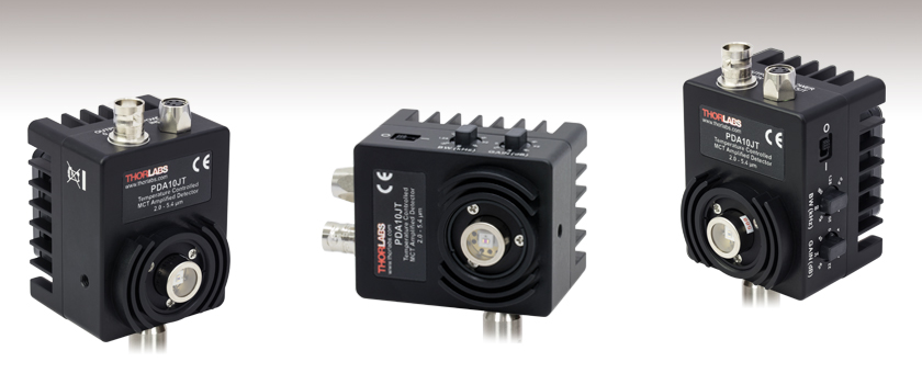
PDA10JT
Post Not Included
Side Mounted,
Post Not Included
PDA10JT
Side View,
Post Not Included
Power Supply
Included with
Detector


Please Wait
| MIR Photodetector Selection Guidea | |||
|---|---|---|---|
| Item # (Detector) | Wavelength Range |
Maximum Bandwidth |
Thermoelectric Cooler |
| PDA10DT (InGaAs) | 0.9 - 2.57 µm | 1,000 kHz | Yes |
| PDA10D2 (InGaAs) | 0.9 - 2.6 µm | 25,000 kHz | No |
| PDA10PT (InAsSb) | 1.0 - 5.8 µm | 1,600 kHz | Yes |
| PDA07P2 (InAsSb) | 2.7 - 5.3 µm | 9 MHz | No |
| PDA10JT (HgCdTe) | 2.0 - 5.4 µm | 160 kHz | Yes |
| PDAVJ8 (HgCdTe) | 2.0 - 8.0 µm | 100 MHz | No |
| PDAVJ10 (HgCdTe) | 2.0 - 10.6 µm | 100 MHz | No |
| PDAVJ5 (HgCdTe) | 2.7 - 5.0 µm | 1 MHz | No |
Features
- Sensitive to Mid-IR (MIR) Light from 2.0 - 5.4 µm
- Max Bandwidth of Detector Package: 160 kHz
- Built-In Thermoelectric Cooler Improves Sensitivity
- 1 mm x 1 mm Detector Element
- Post Mountable in Two Orientations
- Internally SM1 (1.035"-40) Threaded
- Location-Specific Power Adapter Included
Thorlabs' PDA10JT(-EC) Amplified Detector is a thermoelectrically cooled photoconductive HgCdTe (mercury cadmium telluride, MCT) detector. It is sensitive to light in the mid-IR spectral range from 2.0 to 5.4 µm. Two rotary switches control the gain amplifier and detector package bandwidth, allowing performance to be optimized for a variety of applications. The gain switch features eight discrete steps from 0 - 40 dB, while the bandwidth switch provides eight discrete steps from 1.25 - 160 kHz. The thermoelectric cooler (TEC) uses a thermistor feedback loop to hold the temperature of the detector element at -30 °C, minimizing thermal contributions to the output signal.
For best results, we recommend connecting the output cable (not included) to a 50 Ω termination. Because the detector is AC coupled, it requires a pulsed or chopped input signal. AC-coupled detectors will not see unchopped CW light because they are only sensitive to intensity changes, not absolute intensity.

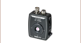
Click to Enlarge
Side View Showing Gain and Bandwidth Adjusters

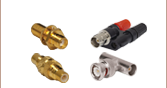
Click to Enlarge
Top View Showing Signal Output and Power Input
The detector package incorporates many of the same mechanical features as our other mounted photodetectors. An internal SM1 (1.035"-40) threading allows Ø1" lens tubes to be mounted in front of the detector element. Two 8-32 (M4 in the -EC version) tapped holes connect a Ø1/2" post to the housing in one of two perpendicular orientations, as shown in the image at the top of the page. The PDA10JT(-EC) includes a 100 - 240 VAC power adapter. If you require a different adapter plug, please contact Tech Support prior to ordering. An SM1RR Retaining Ring is also included.
This detector's output signal depends nonlinearly on the optical input power; for a plot of this, see the Graphs tab. Please note that inhomogeneities at the edges of the active area of the detector can generate unwanted capacitance and resistance effects that distort the time-domain response of the output. Thorlabs therefore recommends that the incident light is well centered on the active area. The SM1 (1.035"-40) threading on the housing can be connected to an SM1 lens tube; the lens tube can be used to mount an iris or pinhole in front of the detector element. Because the detector package protrudes 3.9 mm beyond the front of the threading, optics and optomechanics cannot be attached directly to the housing.
In addition to the HgCdTe detector sold here, Thorlabs manufactures a InAsSb detector with broader wavelength sensitivity and higher bandwidth at the expense of a higher NEP. If a more compact detector housing is desired, we also offer room-temperature amplified photodetectors.
All values given below are for a 50 Ω load, unless otherwise stated.
| Gain (High Z)c | |
|---|---|
| 0 dB | 0.8 V/V |
| 4 dB | 1.6 V/V |
| 10 dB | 3.2 V/V |
| 16 dB | 6.3 V/V |
| 22 dB | 12.6 V/V |
| 28 dB | 25.2 V/V |
| 34 dB | 50.1 V/V |
| 40 dB | 100 V/V |
| Noise-Equivalent Power (NEP) Valuesd | |
|---|---|
| Gain | NEP |
| 0 dB | 1.43 × 10⁻⁹ W/Hz1/2 |
| 4 dB | 7.62 × 10⁻¹⁰ W/Hz1/2 |
| 10 dB | 4.05 × 10⁻¹⁰ W/Hz1/2 |
| 16 dB | 2.78 × 10⁻¹⁰ W/Hz1/2 |
| 22 dB | 2.15 × 10⁻¹⁰ W/Hz1/2 |
| 28 dB | 2.10 × 10⁻¹⁰ W/Hz1/2 |
| 34 dB | 1.97 × 10⁻¹⁰ W/Hz1/2 |
| 40 dB | 1.84 × 10⁻¹⁰ W/Hz1/2 |
| Item # | PDA10JT(-EC) |
|---|---|
| Optical Specifications | |
| Wavelength Range | 2.0 - 5.4 μm |
| Peak Wavelength (λP) | 4.8 μm |
| Peak Responsivity | 300 V/W (Typ.) at Peak Wavelength |
| Electrical Specifications | |
| Gain Settings | 0, 4, 10, 16, 22, 28, 34, 40 dB (8 Steps) |
| Bandwidth Settings | 1.25, 2.5, 5, 10, 20, 40, 80, or 160 kHz (8 Steps) |
| Output Voltagea | 0 - 5 V at 50 Ω 0 - 10 V at High Z |
| Output Impedance | 50 Ω |
| Output Current | 100 mA (Max) |
| Load Impedance | 50 Ω to High Z |
| Output Offsetb | 20 mV (Typ.) 45 mV (Max) |
| Thermoelectric Cooler Specifications | |
| TEC Temperature | -30 °C |
| TEC Current | 0.6 A (Typ.) 1.0 A (Max) |
| Thermistor | 10 kΩ |
| Physical Specifications | |
| Detector Element | HgCdTe (MCT) |
| Active Area | 1 mm × 1 mm |
| Surface Depth | 0.11" ± 0.02" (2.90 ± 0.40 mm) |
| Output | BNC |
| Detector Size | 3" × 2.2" × 2.2" (76.2 mm × 55.9 mm × 55.9 mm) |
| Weight | Detector: 0.42 lbs (191 g) Power Supply: 0.82 lbs (372 g) |
| Power Supply | 27 W, Location-Specific Power Cord Included |
| Input Power | 100 - 240 VAC, 50 - 60 Hz |
| Storage Temperature | 0 to 85 °C |
| Operating Temperature | 0 to 30 °C |


Click to Enlarge
These traces compare the noise level for the lowest gain and bandwidth settings to the noise level for the highest gain and bandwidth settings.

Click to Enlarge
This trace shows that the responsivity varies with input power. For example, increasing the power from 2.5 mW to 5 mW (a difference of 2.5 mW) produces a greater signal change than increasing the power from 25 mW to 27.5 mW (also a difference of 2.5 mW).

Click to Enlarge
The graph above is for the 0 dB gain setting.
Detectivity, D*, is defined as:

where A is the area of the photosensitive region of the detector, Δf is the effective noise bandwidth, and NEP is the noise-equivalent power.
Output Signal
BNC Female

0 - 5 V at 50 Ω
0 - 10 V at High Z
100 mA Max Current
Power Input
4-Pin Female

| Pin | Connection |
|---|---|
| 1 | -12 V |
| 2 | Ground |
| 3 | +5 V |
| 4 | +12 V |
Photodiode Tutorial
Theory of Operation
A junction photodiode is an intrinsic device that behaves similarly to an ordinary signal diode, but it generates a photocurrent when light is absorbed in the depleted region of the junction semiconductor. A photodiode is a fast, highly linear device that exhibits high quantum efficiency based upon the application and may be used in a variety of different applications.
It is necessary to be able to correctly determine the level of the output current to expect and the responsivity based upon the incident light. Depicted in Figure 1 is a junction photodiode model with basic discrete components to help visualize the main characteristics and gain a better understanding of the operation of Thorlabs' photodiodes.


Figure 1: Photodiode Model
Photodiode Terminology
Responsivity
The responsivity of a photodiode can be defined as a ratio of generated photocurrent (IPD) to the incident light power (P) at a given wavelength:

Modes of Operation (Photoconductive vs. Photovoltaic)
A photodiode can be operated in one of two modes: photoconductive (reverse bias) or photovoltaic (zero-bias). Mode selection depends upon the application's speed requirements and the amount of tolerable dark current (leakage current).
Photoconductive
In photoconductive mode, an external reverse bias is applied, which is the basis for our DET series detectors. The current measured through the circuit indicates illumination of the device; the measured output current is linearly proportional to the input optical power. Applying a reverse bias increases the width of the depletion junction producing an increased responsivity with a decrease in junction capacitance and produces a very linear response. Operating under these conditions does tend to produce a larger dark current, but this can be limited based upon the photodiode material. (Note: Our DET detectors are reverse biased and cannot be operated under a forward bias.)
Photovoltaic
In photovoltaic mode the photodiode is zero biased. The flow of current out of the device is restricted and a voltage builds up. This mode of operation exploits the photovoltaic effect, which is the basis for solar cells. The amount of dark current is kept at a minimum when operating in photovoltaic mode.
Dark Current
Dark current is leakage current that flows when a bias voltage is applied to a photodiode. When operating in a photoconductive mode, there tends to be a higher dark current that varies directly with temperature. Dark current approximately doubles for every 10 °C increase in temperature, and shunt resistance tends to double for every 6 °C rise. Of course, applying a higher bias will decrease the junction capacitance but will increase the amount of dark current present.
The dark current present is also affected by the photodiode material and the size of the active area. Silicon devices generally produce low dark current compared to germanium devices which have high dark currents. The table below lists several photodiode materials and their relative dark currents, speeds, sensitivity, and costs.
| Material | Dark Current | Speed | Spectral Range | Cost |
|---|---|---|---|---|
| Silicon (Si) | Low | High Speed | Visible to NIR | Low |
| Germanium (Ge) | High | Low Speed | NIR | Low |
| Gallium Phosphide (GaP) | Low | High Speed | UV to Visible | Moderate |
| Indium Gallium Arsenide (InGaAs) | Low | High Speed | NIR | Moderate |
| Indium Arsenide Antimonide (InAsSb) | High | Low Speed | NIR to MIR | High |
| Extended Range Indium Gallium Arsenide (InGaAs) | High | High Speed | NIR | High |
| Mercury Cadmium Telluride (MCT, HgCdTe) | High | Low Speed | NIR to MIR | High |
Junction Capacitance
Junction capacitance (Cj) is an important property of a photodiode as this can have a profound impact on the photodiode's bandwidth and response. It should be noted that larger diode areas encompass a greater junction volume with increased charge capacity. In a reverse bias application, the depletion width of the junction is increased, thus effectively reducing the junction capacitance and increasing the response speed.
Bandwidth and Response
A load resistor will react with the photodetector junction capacitance to limit the bandwidth. For best frequency response, a 50 Ω terminator should be used in conjunction with a 50 Ω coaxial cable. The bandwidth (fBW) and the rise time response (tr) can be approximated using the junction capacitance (Cj) and the load resistance (RLOAD):

Noise Equivalent Power
The noise equivalent power (NEP) is the generated RMS signal voltage generated when the signal to noise ratio is equal to one. This is useful, as the NEP determines the ability of the detector to detect low level light. In general, the NEP increases with the active area of the detector and is given by the following equation:

Here, S/N is the Signal to Noise Ratio, Δf is the Noise Bandwidth, and Incident Energy has units of W/cm2. For more information on NEP, please see Thorlabs' Noise Equivalent Power White Paper.
Terminating Resistance
A load resistance is used to convert the generated photocurrent into a voltage (VOUT) for viewing on an oscilloscope:

Depending on the type of the photodiode, load resistance can affect the response speed. For maximum bandwidth, we recommend using a 50 Ω coaxial cable with a 50 Ω terminating resistor at the opposite end of the cable. This will minimize ringing by matching the cable with its characteristic impedance. If bandwidth is not important, you may increase the amount of voltage for a given light level by increasing RLOAD. In an unmatched termination, the length of the coaxial cable can have a profound impact on the response, so it is recommended to keep the cable as short as possible.
Shunt Resistance
Shunt resistance represents the resistance of the zero-biased photodiode junction. An ideal photodiode will have an infinite shunt resistance, but actual values may range from the order of ten Ω to thousands of MΩ and is dependent on the photodiode material. For example, and InGaAs detector has a shunt resistance on the order of 10 MΩ while a Ge detector is in the kΩ range. This can significantly impact the noise current on the photodiode. For most applications, however, the high resistance produces little effect and can be ignored.
Series Resistance
Series resistance is the resistance of the semiconductor material, and this low resistance can generally be ignored. The series resistance arises from the contacts and the wire bonds of the photodiode and is used to mainly determine the linearity of the photodiode under zero bias conditions.
Common Operating Circuits

Figure 2: Reverse-Biased Circuit (DET Series Detectors)
The DET series detectors are modeled with the circuit depicted above. The detector is reverse biased to produce a linear response to the applied input light. The amount of photocurrent generated is based upon the incident light and wavelength and can be viewed on an oscilloscope by attaching a load resistance on the output. The function of the RC filter is to filter any high-frequency noise from the input supply that may contribute to a noisy output.

Figure 3: Amplified Detector Circuit
One can also use a photodetector with an amplifier for the purpose of achieving high gain. The user can choose whether to operate in Photovoltaic of Photoconductive modes. There are a few benefits of choosing this active circuit:
- Photovoltaic mode: The circuit is held at zero volts across the photodiode, since point A is held at the same potential as point B by the operational amplifier. This eliminates the possibility of dark current.
- Photoconductive mode: The photodiode is reversed biased, thus improving the bandwidth while lowering the junction capacitance. The gain of the detector is dependent on the feedback element (Rf). The bandwidth of the detector can be calculated using the following:

where GBP is the amplifier gain bandwidth product and CD is the sum of the junction capacitance and amplifier capacitance.
Effects of Chopping Frequency
The photoconductor signal will remain constant up to the time constant response limit. Many detectors, including PbS, PbSe, HgCdTe (MCT), and InAsSb, have a typical 1/f noise spectrum (i.e., the noise decreases as chopping frequency increases), which has a profound impact on the time constant at lower frequencies.
The detector will exhibit lower responsivity at lower chopping frequencies. Frequency response and detectivity are maximized for
![]()
| Posted Comments: | |
madhan2388
(posted 2017-12-20 16:55:39.85) Is there any ways to use this detector for unpulsed/unchopped light? or is there any ways to use this detector without chopper? TIA. YLohia
(posted 2018-03-22 04:04:21.0) Hello, thank you for contacting Thorlabs. These detectors are made using HgCdTe, which is photoconductive. This drowns out the DC signal produced from the CW light with noise. Furthermore, the TIA in the AC-coupled detector packaging contains a DC blocking capacitor. If chopping/modulating your input into the detector is not possible, you could look into our thermal sensors (for e.g., S401C). tcohen
(posted 2012-06-01 09:36:00.0) Response from Tim at Thorlabs: Thank you for your interest! We are often able to provide components individually. I will contact you to discuss the details. stan
(posted 2012-05-31 14:24:17.0) Do you have a way to purchase just the casing for this device? I would like to build a few custom detectors for my lab, but cost of design & machining custom cases is much larger than PCBs. tcohen
(posted 2012-02-24 13:55:00.0) Response from Tim at Thorlabs to Victor: Thank you for your question. Both the PDA10DT and the PDA10JT use Borosilicate glass. victor.karaganov
(posted 2012-02-23 18:04:00.0) Do PDA10DT and PDA10JT have windows? What is the window material? Thorlabs
(posted 2010-07-28 10:32:00.0) Response from Javier at Thorlabs to blee66: Thank you for your feedback. You can certainly amplify the signal from the detector. The disadvantage with multistage designs is that both the signal and noise are amplified. So, you need to take offset into account. In order to reach the 70 dB level, you will need to provide a voltage gain of about 300 V/V. blee66
(posted 2010-07-26 18:33:14.0) This detector would be perfect for me, except that I need to maintain 1 MHz bandwidth at the 70 dB gain setting.
Has anyone tried to further amplify the signal out of this detector? My thought is to leave the detector on the 20 dB setting (where the gain bandwidth is still sufficiently high) and then amplify the output to the needed level.
Any thoughts? zarebagh
(posted 2010-07-18 11:52:49.0) Hi, I would like to know if there is any way to reduce the TEC temp under -10 C. The idea is to improve the SNR! Adam
(posted 2010-05-25 09:15:56.0) A response from Adam at Thorlabs: NEP is the noise floor of a detector, normalized to a 1Hz bandwidth and is expressed in Watts per square root bandwidth. To derive NEP, two parameters must be measured: the detector responsivity at a specified frequency, and the detector voltage noise at the same frequency. Basically the frequency component is removed to make the detectors more comparable. So in the case of the PDA10DT the NEP is a factor of 10 better at the roughly equivalent gain setting (20dB or ~15kV/A) to the PDA10D (10kV/A).
As for the differences between the cooled and uncooled version it is more than just the NEP. The uncooled version is very limited in performance due to high offsets and high NEP. Cooling the detector has a number of effects. First it significantly lowers the dark current offset produced by long wavelength InGaAs detectors. This allows us to add significantly more gain before the dark current offset becomes a problem. Cooling detectors lowers the thermal induced noise. One of the noise sources of these detectors is due to variations in temperature effecting the offset. This appears as additional noise (usually low BW) on the output. By stabilizing the temperature and holding it low enough that the dark current is lower decreases this noise source significantly. Overall the noise performance is significantly better in the PDA10DT as well as the dark current. The addition of the LPF adjustment can lower the noise even more if BW can be limited. user
(posted 2010-05-24 17:04:00.0) Specifications as current shown on your web:
Uncooled PDA10D: DC - 15 MHz 3.5x10^-11 W/Hz^1/2
Cooled PDA10DT: NEP, Max (@ 1 MHz, 0 dB Gain, 50 ?) 2.71 x 10^-11 W/Hz^1/2
Please help me understand your NEP numbers for these two products, in order to calculate the NEP power in Watts at 1 MHz i multiply both numbers by SQRT(10^6), but you indicate the NEP data point for the cooled sensor is valid "@ 1 MHz". I guess you really mean DC to 1 MHz, please confirm. The reason i am so focused here is the model with cooling has a roughly 25% better NEP than the one without, seems like a big price to pay for such a small improvement in NEP. Adam
(posted 2010-04-27 12:07:03.0) A response from Adam at Thorlabs to sking: The current diode that is used in the PDA10DT is not designed for use below 1um and we do not have response information below 1.2um. I will send you the extra data that we can provide via email. sking
(posted 2010-04-27 11:06:06.0) Does the detector have any respnse below the 1um which you specify on the spec sheet? Do you have the product details for the actaul photodoiode in the detector e.g.hamamatsu etc... klee
(posted 2009-08-13 16:49:00.0) A response from Ken at Thorlabs to dedeianc: The rise time depends on the gain and filter settings. Since there are 8 gain settings and 8 filter settings, there are 64 gain/filter combinations and rise time is different for each combination. The risetime however can be approximated to tr = 0.35/BW and the maximum bandwidth for the PDA10DT is 1MHz. dedeianc
(posted 2009-08-13 11:38:21.0) By time resolution I mean rise time klee
(posted 2009-08-13 10:09:56.0) A response from Ken at Thorlabs to dedeianc: Please explain what you mean by "time resolution". dedeianc
(posted 2009-08-11 11:41:44.0) What is the time resolution of these detectors klee
(posted 2009-07-09 11:11:00.0) A response from Ken at Thorlabs to Crice: We do not have CW saturation or damage threshold. Although CW saturations is in the range of 1-2mW as a safe number. For the NEP, there are numerous combinations with 8 gain steps and 8 possible LPF setting for each. We do provide the noise in graphs, worst to best case. crice
(posted 2009-07-05 20:07:29.0) What is the NEP (Jones), CW Saturation (Watts), and Damage Threshold (Watts) for this detector? klee
(posted 2009-06-23 11:13:56.0) A response from Ken at Thorlabs to xindoutoya: These detectors only have voltage output through the BNC connector. There is no USB or any other digital signal output. xindoutoya
(posted 2009-06-23 01:15:41.0) I have a question about "Extended Range InGaAs Detectors": is there a USB connection cable between the product and a computer?
Please reply to me as soon as possible. Thanks very much. |
The following table lists Thorlabs' selection of photodiodes and photoconductive detectors. Item numbers in the same row contain the same detector element.
| Photodetector Cross Reference | ||||||
|---|---|---|---|---|---|---|
| Wavelength | Material | Unmounted Photodiode |
Unmounted Photoconductor |
Mounted Photodiode |
Biased Detector |
Amplified Detector |
| 150 - 550 nm | GaP | - | - | SM05PD7A | DET25K2 | PDA25K2 |
| 200 - 1100 nm | Si | FDS010 | - | SM05PD2A SM05PD2B |
DET10A2 | PDA10A2 |
| Si | - | - | SM1PD2A | - | - | |
| 320 - 1000 nm | Si | - | - | - | - | PDA8A2 |
| 320 - 1100 nm | Si | FD11A | SM05PD3A | PDF10A2 | ||
| Si | - | - | - | DET100A2 | PDA100A2 | |
| 340 - 1100 nm | Si | FDS10X10 | - | - | - | - |
| 350 - 1100 nm | Si | FDS100 FDS100-CAL a |
- | SM05PD1A SM05PD1B |
DET36A2 | PDA36A2 |
| Si | FDS1010 FDS1010-CAL a |
- | SM1PD1A SM1PD1B |
- | - | |
| 400 - 1000 nm | Si | - | - | - | - | PDA015A(/M) FPD310-FS-VIS FPD310-FC-VIS FPD510-FC-VIS FPD510-FS-VIS FPD610-FC-VIS FPD610-FS-VIS |
| 400 - 1100 nm | Si | FDS015 b | - | - | - | - |
| Si | FDS025 b FDS02 c |
- | - | DET02AFC(/M) DET025AFC(/M) DET025A(/M) DET025AL(/M) |
- | |
| 400 - 1700 nm | Si & InGaAs | DSD2 | - | - | - | - |
| 500 - 1700 nm | InGaAs | - | - | - | DET10N2 | - |
| 750 - 1650 nm | InGaAs | - | - | - | - | PDA8GS |
| 800 - 1700 nm | InGaAs | FGA015 | - | - | - | PDA015C(/M) |
| InGaAs | FGA21 FGA21-CAL a |
- | SM05PD5A | DET20C2 | PDA20C2 PDA20CS2 |
|
| InGaAs | FGA01 b FGA01FC c |
- | - | DET01CFC(/M) | - | |
| InGaAs | FDGA05 b | - | - | - | PDA05CF2 | |
| InGaAs | - | - | - | DET08CFC(/M) DET08C(/M) DET08CL(/M) |
PDF10C/M | |
| 800 - 1800 nm | Ge | FDG03 FDG03-CAL a |
- | SM05PD6A | DET30B2 | PDA30B2 |
| Ge | FDG50 | - | - | DET50B2 | PDA50B2 | |
| Ge | FDG05 | - | - | - | - | |
| 900 - 1700 nm | InGaAs | FGA10 | - | SM05PD4A | DET10C2 | PDA10CS2 |
| 900 - 2600 nm | InGaAs | FD05D | - | - | DET05D2 | - |
| FD10D | - | - | DET10D2 | PDA10D2 | ||
| 950 - 1650 nm | InGaAs | - | - | - | - | FPD310-FC-NIR FPD310-FS-NIR FPD510-FC-NIR FPD510-FS-NIR FPD610-FC-NIR FPD610-FS-NIR |
| 1.0 - 5.8 µm | InAsSb | - | - | - | - | PDA10PT(-EC) |
| 2.0 - 5.4 µm | HgCdTe (MCT) | - | - | - | - | PDA10JT(-EC) |
| 2.0 - 8.0 µm | HgCdTe (MCT) | VML8T0 VML8T4 d |
- | - | - | PDAVJ8 |
| 2.0 - 10.6 µm | HgCdTe (MCT) | VML10T0 VML10T4 d |
- | - | - | PDAVJ10 |
| 2.7 - 5.0 µm | HgCdTe (MCT) | VL5T0 | - | - | - | PDAVJ5 |
| 2.7 - 5.3 µm | InAsSb | - | - | - | - | PDA07P2 |