 Products Home
HgCdTe (MCT) Amplified Photodetectors
- HgCdTe (MCT) Detectors with Optically Immersed Sensors
- Three Models Available Covering 2.0 to 10.6 µm
- Adjustable Gain Selection
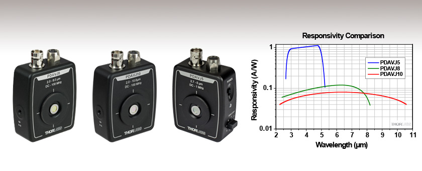
PDAVJ8
2.0 - 8.0 µm,
DC to 100 MHz
PDAVJ10
2.0 - 10.6 µm,
DC to 100 MHz
PDAVJ5
2.7 - 5.0 µm,
DC to 1 MHz


Please Wait
| MIR Photodetector Selection Guidea | |||
|---|---|---|---|
| Item # (Detector) | Wavelength Range |
Maximum Bandwidth |
Thermoelectric Cooler |
| PDA10DT (InGaAs) | 0.9 - 2.57 µm | 1,000 kHz | Yes |
| PDA10D2 (InGaAs) | 0.9 - 2.6 µm | 25,000 kHz | No |
| PDA10PT (InAsSb) | 1.0 - 5.8 µm | 1,600 kHz | Yes |
| PDA07P2 (InAsSb) | 2.7 - 5.3 µm | 9 MHz | No |
| PDA10JT (HgCdTe) | 2.0 - 5.4 µm | 160 kHz | Yes |
| PDAVJ8 (HgCdTe) | 2.0 - 8.0 µm | 100 MHz | No |
| PDAVJ10 (HgCdTe) | 2.0 - 10.6 µm | 100 MHz | No |
| PDAVJ5 (HgCdTe) | 2.7 - 5.0 µm | 1 MHz | No |

Click for Details
A hyperhemispherical lens forms an image on a virtual plane behind the sensor element, resulting in an effective optical area greater than the physical sensor area.

Click for Details
A standard hemispherical immersion lens forms an image in the plane of the sensor element.
Features
- Photovoltaic Detectors Sensitive to MIR Light:
- PDAVJ8: 2.0 - 8.0 µm
- PDAVJ10: 2.0 - 10.6 µm
- PDAVJ5: 2.7 - 5.0 µm
- High Bandwidth:
- PDAVJ8: True DC - 100 MHz
- PDAVJ10: True DC - 100 MHz
- PDAVJ5: True DC - 1 MHz
- Effective Detector Area: 1 mm2 (1 mm x 1 mm)
- Post Mountable in Two Orientations Using Universal 8-32 & M4 Tapped Holes
- External SM1 (1.035"-40) Threads and Internal SM05 (0.535"-40) Threads
- Location-Specific Power Adapter Included
Thorlabs' Amplified HgCdTe (mercury cadmium telluride, MCT) Photovoltaic Detectors are sensitive to MIR light. A rotary switch controls the gain amplifier (shown in the photo below), allowing performance to be optimized for a variety of applications. The gain switch features eight discrete steps from 0 to 30 dB (Item #s PDAVJ8 and PDAVJ10) or 0 to 42 dB (Item # PDAVJ5). For best results, we recommend connecting the output cable (not included) to a 50 Ω termination.
Each HgCdTe (MCT) sensor element is integrated with a hyperhemispherical GaAs lens to achieve optical immersion, and each detector is provided with a wedged ZnSe window that is AR-coated for the 2 - 13 µm wavelength range.

Click to Enlarge
Side View Showing Gain Adjuster
The detector package incorporates many of the same mechanical features as our other mounted photodetectors. External SM1 (1.035"-40) and internal SM05 (0.535"-40) threading allows Ø1" lens tubes or Ø1/2" lens tubes to be mounted in front of the detector element. Universal 8-32 & M4 tapped holes connect a Ø1/2" post to the housing in one of two perpendicular orientations. A location-specific power supply is included with each detector.
Optically Immersed Sensor Element
Optical Immersion is used in these MCT detectors to produce a 1 mm2 effective detector area, approximately two orders of magnitude larger than the actual sensor, resulting in increased responsivity and reduced capacitance. This technique is performed by integrating the sensor element with a GaAs hyperhemispherical microlens, which has a high refractive index (n = 3.3) and is transparent to MIR wavelengths. The diagrams to the right illustrate the benefit of using a hyperhemispherical lens, rather than a hemispherical lens. A hemispherical lens focuses light onto the sensor plane (left diagram) and produces an image with dimensions larger than the physical sensor by a factor of n. The hyperhemispherical lens (right diagram) forms an image on a virtual focal plane located behind the sensor, and this image has dimensions larger than the physical sensor by a factor of n2. Note that the acceptance angle is reduced to 35° by the hyperhemispherical lens, in contrast to the 180° acceptance angle that would be obtained if a hemispherical lens were used.
All specifications are valid at 23 ± 5°C and 45 ± 15% relative humidity.
| Item # | PDAVJ8 | PDAVJ10 | PDAVJ5 |
|---|---|---|---|
| Optical Specifications | |||
| Wavelength Range | 2.0 - 8.0 μm | 2.0 - 10.6 μm | 2.7 - 5.0 μm |
| Peak Wavelength (λP) | 6.5 μm | 6.5 μm | 4.75 μm |
| Window Material | ZnSe | ||
| Saturation Input Power | 250 µW | 500 µW | 200 µW |
| Max Input Power (Photodiode Damage Threshold) |
CW or >1 µs Pulse: 2.5 W/cm2 <1 µs Pulse: 10 kW/cm2 |
||
| Electrical Specifications | |||
| Responsivity × Effective Detector Width @ λP | ≥0.04 A·mm/Wa | ≥0.01 A·mm/Wa | - |
| Current Responsivity @ λP | - | - | ≥1 A/W |
| Detectivity (D*) @ λP | ≥6.0×108 cm·Hz1/2·W-1 | ≥2.0×108 cm·Hz1/2·W-1 | ≥1.5×1010 cm·Hz1/2·W-1 |
| Gain Adjustment Range | 30 dB | 30 dB | 42 dB |
| Gain Steps | 8 | ||
| Conversion Gain @ Gain = 8, λP | 6000 V/W | 4000 V/W | 200 000 V/W |
| Conversion Gain @ Gain = 1, λP | 185 V/W | 120 V/W | 1500 V/W |
| Output Bandwidth (3 dB) | DC - 100 MHzb | DC - 100 MHzb | DC - 1 MHzc |
| Noise Equivalent Power (NEP)d | 170 pW/Hz1/2 | 210 pW/Hz1/2 | 14 pW/Hz1/2 |
| Output Voltage (Max) | 0 - 1.0 V (50 Ω) 0 - 2.0 V (Hi-Z) |
||
| Output Impedance | BNC, 50 Ω | ||
| Output Current (Max) | 50 mA | ||
| Output Offset Voltage | <±25 mV | ||
| General Specifications | |||
| Optical Input | Free Space | ||
| Electrical Output | BNC | ||
| Detector Element | HgCdTe (MCT), Optically Immersed | ||
| Effective Detector Size | 1 mm x 1 mm, Multilayer | 1 mm x 1 mm, Multilayer | 1 mm x 1 mm, Single Layer |
| Housing Dimensions | 70.9 mm × 54.1 mm × 22.5 mm (2.79" × 2.13" × 0.89") |
||
| Depth of Detector Surfacee | 4.3 mm | ||
| Depth of Protective Windowe | 1.1 mm | ||
| Weight | Detector: 0.18 lbs (80 g) Power Supply: 0.9 lbs (400 g) |
||
| Included Power Supply | ±12 V @ 250 mA (100/120/230 VAC, 50 - 60 Hz, Switchable) |
||
| Operating Temperature | 15 to 30 °C | ||
| Storage Temperature | 0 to 45 °C | ||
Output Signal
BNC Female

0 - 1.0 V at 50 Ω
0 - 2.0 V at High Z
50 mA Max Current
Power Input
3-Pin Female

Photodiode Tutorial
Theory of Operation
A junction photodiode is an intrinsic device that behaves similarly to an ordinary signal diode, but it generates a photocurrent when light is absorbed in the depleted region of the junction semiconductor. A photodiode is a fast, highly linear device that exhibits high quantum efficiency based upon the application and may be used in a variety of different applications.
It is necessary to be able to correctly determine the level of the output current to expect and the responsivity based upon the incident light. Depicted in Figure 1 is a junction photodiode model with basic discrete components to help visualize the main characteristics and gain a better understanding of the operation of Thorlabs' photodiodes.


Figure 1: Photodiode Model
Photodiode Terminology
Responsivity
The responsivity of a photodiode can be defined as a ratio of generated photocurrent (IPD) to the incident light power (P) at a given wavelength:

Modes of Operation (Photoconductive vs. Photovoltaic)
A photodiode can be operated in one of two modes: photoconductive (reverse bias) or photovoltaic (zero-bias). Mode selection depends upon the application's speed requirements and the amount of tolerable dark current (leakage current).
Photoconductive
In photoconductive mode, an external reverse bias is applied, which is the basis for our DET series detectors. The current measured through the circuit indicates illumination of the device; the measured output current is linearly proportional to the input optical power. Applying a reverse bias increases the width of the depletion junction producing an increased responsivity with a decrease in junction capacitance and produces a very linear response. Operating under these conditions does tend to produce a larger dark current, but this can be limited based upon the photodiode material. (Note: Our DET detectors are reverse biased and cannot be operated under a forward bias.)
Photovoltaic
In photovoltaic mode the photodiode is zero biased. The flow of current out of the device is restricted and a voltage builds up. This mode of operation exploits the photovoltaic effect, which is the basis for solar cells. The amount of dark current is kept at a minimum when operating in photovoltaic mode.
Dark Current
Dark current is leakage current that flows when a bias voltage is applied to a photodiode. When operating in a photoconductive mode, there tends to be a higher dark current that varies directly with temperature. Dark current approximately doubles for every 10 °C increase in temperature, and shunt resistance tends to double for every 6 °C rise. Of course, applying a higher bias will decrease the junction capacitance but will increase the amount of dark current present.
The dark current present is also affected by the photodiode material and the size of the active area. Silicon devices generally produce low dark current compared to germanium devices which have high dark currents. The table below lists several photodiode materials and their relative dark currents, speeds, sensitivity, and costs.
| Material | Dark Current | Speed | Spectral Range | Cost |
|---|---|---|---|---|
| Silicon (Si) | Low | High Speed | Visible to NIR | Low |
| Germanium (Ge) | High | Low Speed | NIR | Low |
| Gallium Phosphide (GaP) | Low | High Speed | UV to Visible | Moderate |
| Indium Gallium Arsenide (InGaAs) | Low | High Speed | NIR | Moderate |
| Indium Arsenide Antimonide (InAsSb) | High | Low Speed | NIR to MIR | High |
| Extended Range Indium Gallium Arsenide (InGaAs) | High | High Speed | NIR | High |
| Mercury Cadmium Telluride (MCT, HgCdTe) | High | Low Speed | NIR to MIR | High |
Junction Capacitance
Junction capacitance (Cj) is an important property of a photodiode as this can have a profound impact on the photodiode's bandwidth and response. It should be noted that larger diode areas encompass a greater junction volume with increased charge capacity. In a reverse bias application, the depletion width of the junction is increased, thus effectively reducing the junction capacitance and increasing the response speed.
Bandwidth and Response
A load resistor will react with the photodetector junction capacitance to limit the bandwidth. For best frequency response, a 50 Ω terminator should be used in conjunction with a 50 Ω coaxial cable. The bandwidth (fBW) and the rise time response (tr) can be approximated using the junction capacitance (Cj) and the load resistance (RLOAD):

Noise Equivalent Power
The noise equivalent power (NEP) is the generated RMS signal voltage generated when the signal to noise ratio is equal to one. This is useful, as the NEP determines the ability of the detector to detect low level light. In general, the NEP increases with the active area of the detector and is given by the following equation:

Here, S/N is the Signal to Noise Ratio, Δf is the Noise Bandwidth, and Incident Energy has units of W/cm2. For more information on NEP, please see Thorlabs' Noise Equivalent Power White Paper.
Terminating Resistance
A load resistance is used to convert the generated photocurrent into a voltage (VOUT) for viewing on an oscilloscope:

Depending on the type of the photodiode, load resistance can affect the response speed. For maximum bandwidth, we recommend using a 50 Ω coaxial cable with a 50 Ω terminating resistor at the opposite end of the cable. This will minimize ringing by matching the cable with its characteristic impedance. If bandwidth is not important, you may increase the amount of voltage for a given light level by increasing RLOAD. In an unmatched termination, the length of the coaxial cable can have a profound impact on the response, so it is recommended to keep the cable as short as possible.
Shunt Resistance
Shunt resistance represents the resistance of the zero-biased photodiode junction. An ideal photodiode will have an infinite shunt resistance, but actual values may range from the order of ten Ω to thousands of MΩ and is dependent on the photodiode material. For example, and InGaAs detector has a shunt resistance on the order of 10 MΩ while a Ge detector is in the kΩ range. This can significantly impact the noise current on the photodiode. For most applications, however, the high resistance produces little effect and can be ignored.
Series Resistance
Series resistance is the resistance of the semiconductor material, and this low resistance can generally be ignored. The series resistance arises from the contacts and the wire bonds of the photodiode and is used to mainly determine the linearity of the photodiode under zero bias conditions.
Common Operating Circuits

Figure 2: Reverse-Biased Circuit (DET Series Detectors)
The DET series detectors are modeled with the circuit depicted above. The detector is reverse biased to produce a linear response to the applied input light. The amount of photocurrent generated is based upon the incident light and wavelength and can be viewed on an oscilloscope by attaching a load resistance on the output. The function of the RC filter is to filter any high-frequency noise from the input supply that may contribute to a noisy output.

Figure 3: Amplified Detector Circuit
One can also use a photodetector with an amplifier for the purpose of achieving high gain. The user can choose whether to operate in Photovoltaic of Photoconductive modes. There are a few benefits of choosing this active circuit:
- Photovoltaic mode: The circuit is held at zero volts across the photodiode, since point A is held at the same potential as point B by the operational amplifier. This eliminates the possibility of dark current.
- Photoconductive mode: The photodiode is reversed biased, thus improving the bandwidth while lowering the junction capacitance. The gain of the detector is dependent on the feedback element (Rf). The bandwidth of the detector can be calculated using the following:

where GBP is the amplifier gain bandwidth product and CD is the sum of the junction capacitance and amplifier capacitance.
Effects of Chopping Frequency
The photoconductor signal will remain constant up to the time constant response limit. Many detectors, including PbS, PbSe, HgCdTe (MCT), and InAsSb, have a typical 1/f noise spectrum (i.e., the noise decreases as chopping frequency increases), which has a profound impact on the time constant at lower frequencies.
The detector will exhibit lower responsivity at lower chopping frequencies. Frequency response and detectivity are maximized for
![]()
| Posted Comments: | |
daniel.cremons
(posted 2018-09-06 17:50:29.52) I have the PDAVJ8 and when using the power supply in the 115 V mode (to match my supply; I'm in the US), I see a 30 MHz sawtooth in the signal which is about 20 mV at 0 gain. When I switch the power supply to the 230 V setting the sawtooth goes away and the detector seems to be operating as normal. Could my power supply have gotten the settings switched or is there some other cause of the sawtooth? nreusch
(posted 2018-09-27 09:38:22.0) This is a response from Nicola at Thorlabs. Thank you for your inquiry. We could not reproduce the 30 MHz saw tooth, so there might be an issue with the PSU. As you have not selected “Contact Me” in the feedback form, please get in contact with your local Thorlabs Tech Support team for troubleshooting. |
The following table lists Thorlabs' selection of photodiodes and photoconductive detectors. Item numbers in the same row contain the same detector element.
| Photodetector Cross Reference | ||||||
|---|---|---|---|---|---|---|
| Wavelength | Material | Unmounted Photodiode |
Unmounted Photoconductor |
Mounted Photodiode |
Biased Detector |
Amplified Detector |
| 150 - 550 nm | GaP | - | - | SM05PD7A | DET25K2 | PDA25K2 |
| 200 - 1100 nm | Si | FDS010 | - | SM05PD2A SM05PD2B |
DET10A2 | PDA10A2 |
| Si | - | - | SM1PD2A | - | - | |
| 320 - 1000 nm | Si | - | - | - | - | PDA8A2 |
| 320 - 1100 nm | Si | FD11A | SM05PD3A | PDF10A2 | ||
| Si | - | - | - | DET100A2 | PDA100A2 | |
| 340 - 1100 nm | Si | FDS10X10 | - | - | - | - |
| 350 - 1100 nm | Si | FDS100 FDS100-CAL a |
- | SM05PD1A SM05PD1B |
DET36A2 | PDA36A2 |
| Si | FDS1010 FDS1010-CAL a |
- | SM1PD1A SM1PD1B |
- | - | |
| 400 - 1000 nm | Si | - | - | - | - | PDA015A(/M) FPD310-FS-VIS FPD310-FC-VIS FPD510-FC-VIS FPD510-FS-VIS FPD610-FC-VIS FPD610-FS-VIS |
| 400 - 1100 nm | Si | FDS015 b | - | - | - | - |
| Si | FDS025 b FDS02 c |
- | - | DET02AFC(/M) DET025AFC(/M) DET025A(/M) DET025AL(/M) |
- | |
| 400 - 1700 nm | Si & InGaAs | DSD2 | - | - | - | - |
| 500 - 1700 nm | InGaAs | - | - | - | DET10N2 | - |
| 750 - 1650 nm | InGaAs | - | - | - | - | PDA8GS |
| 800 - 1700 nm | InGaAs | FGA015 | - | - | - | PDA015C(/M) |
| InGaAs | FGA21 FGA21-CAL a |
- | SM05PD5A | DET20C2 | PDA20C2 PDA20CS2 |
|
| InGaAs | FGA01 b FGA01FC c |
- | - | DET01CFC(/M) | - | |
| InGaAs | FDGA05 b | - | - | - | PDA05CF2 | |
| InGaAs | - | - | - | DET08CFC(/M) DET08C(/M) DET08CL(/M) |
PDF10C/M | |
| 800 - 1800 nm | Ge | FDG03 FDG03-CAL a |
- | SM05PD6A | DET30B2 | PDA30B2 |
| Ge | FDG50 | - | - | DET50B2 | PDA50B2 | |
| Ge | FDG05 | - | - | - | - | |
| 900 - 1700 nm | InGaAs | FGA10 | - | SM05PD4A | DET10C2 | PDA10CS2 |
| 900 - 2600 nm | InGaAs | FD05D | - | - | DET05D2 | - |
| FD10D | - | - | DET10D2 | PDA10D2 | ||
| 950 - 1650 nm | InGaAs | - | - | - | - | FPD310-FC-NIR FPD310-FS-NIR FPD510-FC-NIR FPD510-FS-NIR FPD610-FC-NIR FPD610-FS-NIR |
| 1.0 - 5.8 µm | InAsSb | - | - | - | - | PDA10PT(-EC) |
| 2.0 - 5.4 µm | HgCdTe (MCT) | - | - | - | - | PDA10JT(-EC) |
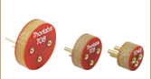
| 2.0 - 8.0 µm | HgCdTe (MCT) | VML8T0 VML8T4 d |
- | - | - | PDAVJ8 |
| 2.0 - 10.6 µm | HgCdTe (MCT) | VML10T0 VML10T4 d |
- | - | - | PDAVJ10 |
| 2.7 - 5.0 µm | HgCdTe (MCT) | VL5T0 | - | - | - | PDAVJ5 |
| 2.7 - 5.3 µm | InAsSb | - | - | - | - | PDA07P2 |
| Item #a,b | Housing Featuresc |
Wavelength Range (λP) |
Responsivity × Effective Detector Width @ λP |
Responsivity @ λP |
Output Bandwidth @ 3 dB |
Conversion Gain @ λP |
NEPd | Typical Performance Graphse |
|---|---|---|---|---|---|---|---|---|
| PDAVJ8 |  |
2.0 - 8.0 µm (6.5 µm) |
≥0.04 A·mm/Wf | - | DC - 100 MHzg | 185 V/W (Gain Setting 1) 6000 V/W (Gain Setting 8) |
170 pW/Hz1/2 | |
| PDAVJ10 | |
2.0 - 10.6 µm (6.5 µm) |
≥0.01 A·mm/Wf | - | DC - 100 MHzg | 120 V/W (Gain Setting 1) 4000 V/W (Gain Setting 8) |
210 pW/Hz1/2 | |
| PDAVJ5 | |
2.7 - 5.0 µm (4.75 µm) |
- | ≥1 A/W | DC - 1 MHzh | 1500 V/W (Gain Setting 1) 200 000 V/W (Gain Setting 8) |
14 pW/Hz1/2 |