 Products Home
Large-Area Balanced Amplified Photodetectors
- Wavelengths Covering the 190 - 1700 nm Range
- Detectors with Diameters up to 5 mm
- Excellent Common Mode Rejection
- Direct Monitor Outputs
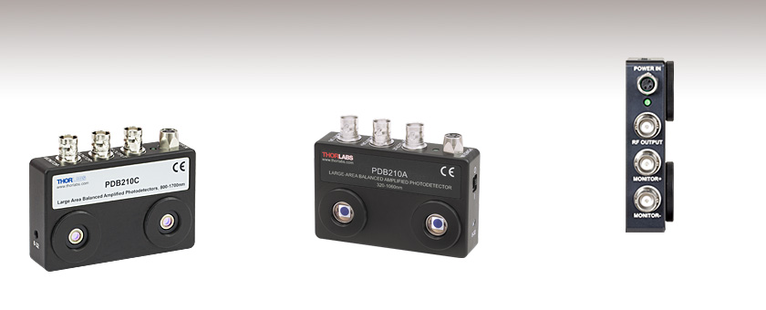
PDB210C
InGaAs Photodetector
for 800 - 1700 nm
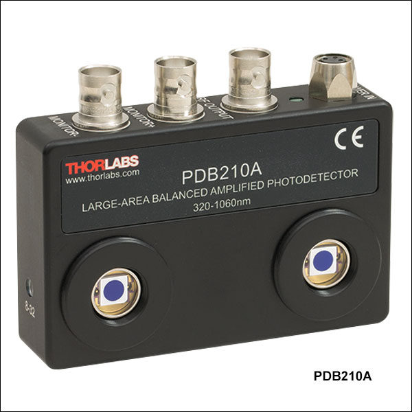
PDB210A
Si Photodetector
for 320 - 1060 nm
Top Panel of
the PDB210A


Please Wait
| Balanced Detector Selection Guide |
|---|
| Balanced Detectors with Fast Monitor Output |
| Large-Area Balanced Amplified Detectors |
| Suitable for OCT |
| Compact Balanced Amplified Detectors |
| Compact 5 GHz Balanced Detectors |
| OCT Balanced Detectors with Fast Monitor Output |
| Auto-Balanced Detector with Avalanche Photodiodes |
| Polarization-Dependent Balanced Detector |
Typical Applications
- Spectroscopy
- Heterodyne Detection
- Optical Coherence Tomography
- Optical Delay Measurements
- THz Detection

Click to Enlarge
Simplified Mechanical Drawing of the PDB220A2 Photodetector
Features
- Large Active Areas for Free-Space Beams
- Three Models
- 190 - 1100 nm (UV-Enhanced Si)
- 320 - 1060 nm (Si)
- 800 - 1700 nm (InGaAs)
- Common Mode Rejection Ratio ≥ 30 dB
- High Bandwidth: DC to 1 MHz
- Ultra Low Noise (See the Specs tab for Model-Specific NEPs)
- Designed for Free-Space Applications (Fiber Input Also Feasible)
- Direct Detector Monitor Outputs
- Includes Swithchable Power Supply
- External SM1 (1.035"-40) Threads and Internal SM05 (0.535"-40) Threads
These Balanced Amplified Photodetectors acts as a balanced receiver by subtracting the two optical input signals from each other, resulting in the cancellation of common mode noise. This allows small changes in the signal path to be extracted from the interfering noise floor.
Each detector uses two well-matched large-area Si or InGaAs detectors and an ultra-low-noise transimpedance amplifier for improved noise reduction. An output voltage (RF-OUTPUT) is generated that is proportional to the difference between the photocurrents in the two photodiodes (i.e., the two optical input signals). Please see the Operation tab for more details. Additionally, the unit has two fast monitor outputs (MONITOR+ and MONITOR-) to measure optical input power levels as well as RF modulated signals on each detector.
The detectors are spaced 2" apart, making beam alignment an easy task on an optical table. To further simplify the use of these detectors, the housing has external SM1 (1.035"-40) and internal SM05 (0.535"-40) threads around each detector to attach components such as lens tubes, cage systems, mounted optics, and fiber collimator adapters. For compatibility with other externally SM1-threaded items, two SM1T1 adapters are included with each detector.
Electrical Connectors
Three BNC electrical connectors provide the balanced output signal plus a power monitor for each of the two input signals. These two monitors can be used as an independent power meter for each channel, which is helpful when adjusting the power level incident on each photodiode.
Packaging/Power Supply
These balanced detectors are housed in a rugged, shielded aluminum enclosure. The housing allows a mounting post adapter to be fixed to the bottom or side surface by 8-32 (M4) screws. The unit is powered from an included ±12 V DC power supply that has an input voltage of 115 V or 230 V that can be manually selected by a switch. A replacement power supply, available below, can support input voltages of 100, 120, and 230 VAC.
Thorlabs also offers Fiber-Based Interferometers, which feature an integrated balanced detector.
| Item # | PDB220A2(/M) | PDB210A(/M) | PDB210C(/M) |
|---|---|---|---|
| Detector Type | UV Enhanced Si/PIN | Si/PIN | InGaAs/PIN |
| Wavelength Range | 190 - 1100 nm | 320 - 1060 nm | 800 - 1700 nm |
| Typical Maximum Responsivity | 0.5 A/W @ 960 nm | 0.6 A/W @ 920 nm | 1.0 A/W @ 1550 nm |
| Active Detector Diameter | 4.1 mm | 5 mm | 3 mm |
| Bandwidth (3 dB) | DC - 1 MHz | ||
| Common Mode Rejection Ratio | 30 dB (Min) 40 dB (Typical) |
40 dB | 30 dB |
| Transimpedance Gain | 500 x 103 V/A 175 x 103 V/A with 50 Ω Termination |
||
| Conversion Gain RF-Output | 250 x 103 V/W 85 x 103 V/W with 50 Ω Termination |
300 x 103 V/W 100 x 103 V/W with 50 Ω Termination |
500 x 103 V/W 175 x 103 V/W with 50 Ω Termination |
| CW Saturation Power RF-Output | 36 µW @ 960 nm | 33 µW @ 920 nm | 20 µW @ 1550 nm |
| Voltage Swing RF-Output | 10 V (Max) 3.5 V (Max with with 50 Ω Termination) |
||
| Conversion Gain Monitor Outputs | 10 V/mW @ 960 nm 1.5 V/mW @ 960 nm with 50 Ω Termination |
10 V/mW @ 920 nm 1.5 V/mW @ 920 nm with 50 Ω Termination |
10 V/mW @ 1550 nm 1.5 V/mW @ 1550 nm with 50 Ω Termination |
| Voltage Swing Monitor Outputs (Max) |
10 V (High Z) 1.5 V (50 Ω) |
||
| Minimum NEP (DC - 1 MHz) | 3.6 pW/√Hz | 2.2 pW/√Hz | 16 pW/√Hz |
| Optical Inputs | Free Space | ||
| Photodiode Damage Threshold | 20 mW | ||
| Electrical Outputs | BNC, 100 Ω | ||
| RF-Output Coupling | DC (AC-Coupling Available upon Request) | ||
| Operating Temperature Rangea | 0 to 40 °C | ||
| Storage Temperature Range | -40 to 70 °C | ||
| Dimensionsb (W x H x L) | 83.8 mm x 65.3 mm x 21.1 mm (3.30" x 2.57" x 0.83") | ||
| Weight | 0.15 kg (w/o Power Supply) | ||
| Included Power Supplyc | ±12 V @ 250 mA (100/120/230 VAC, 50 - 60 Hz, Switchable) |
||
PDB220A2 Balanced Amplified Photodetector (UV-Enhanced Si)


Click to Enlarge
For this measurement, the inputs of the balanced detectors were blocked and the spectra were measured using an electrical spectrum analyzer. The blue "reference" line was measured with the PDB220A2 switched off and is representative of the system's noise floor. The red line marked PDB220A2 was measured with the detector turned on.

Click to Enlarge
Typical RF output frequency response for the PDB220A2.
CMRR indicates the common mode rejection ratio.

Click to Enlarge
Typical frequency response of the PDB220A2 monitor outputs.
PDB210A Balanced Amplified Photodetector (Si)


Click to Enlarge
For this measurement, the inputs of the balanced detectors were blocked and the spectra were measured using an electrical spectrum analyzer. The blue "reference" line was measured with the PDB210A switched off and is representative of the system's noise floor. The red line marked PDB210A was measured with the detector turned on.

Click to Enlarge
Typical RF output frequency response for the PDB210A.
CMRR indicates the common mode rejection ratio.

Click to Enlarge
Typical frequency response of the PDB210A monitor outputs.
PDB210C Balanced Amplified Photodetector (InGaAs)


Click to Enlarge
For this measurement, the inputs of the balanced detectors were blocked and the spectra were measured using an electrical spectrum analyzer. The blue "reference" line was measured with the PDB210C switched off and is representative of the system's noise floor. The red line marked PDB210C was measured with the detector turned on.

Click to Enlarge
Typical RF output frequency response for the PDB210C.
CMRR indicates common mode rejection ratio.

Click to Enlarge
Typical frequency response of the PDB210C monitor outputs.
Pin Diagrams for Large-Area Balanced Amplified Photodetectors
Monitor +/-
BNC Female

0 - 10 V Hi-Z (1.5 V for 50 Ω loads)
RF Output
BNC Female
±10 V for Hi-Z (±3 V for 50 Ω loads)
PDB Male (Power Cables)

PDB Female (Photodetector)

Thorlabs' Large-Area Balanced Amplified Photodetectors consist of two well-matched photodiodes and an ultra-low noise, high-speed transimpedance amplifier (TIA) that generates an output voltage (RF OUTPUT) proportional to the difference between the photocurrents in the two photodiode (i.e., the two optical input signals). Additionally, the unit has two monitor outputs (MONITOR+ and MONITOR-) to observe the optical input power levels on each photodiode.

The following parts are included together with each of our Balanced Amplified Photodetectors:
- Balanced Amplified Photodetector
- 2 SM1T1 Internally SM1-Threaded Adapters
- 2 Metal Cover Caps (for the Input Apertures)
- Power Supply
- Operating Manual
Photodiode Tutorial
Theory of Operation
A junction photodiode is an intrinsic device that behaves similarly to an ordinary signal diode, but it generates a photocurrent when light is absorbed in the depleted region of the junction semiconductor. A photodiode is a fast, highly linear device that exhibits high quantum efficiency based upon the application and may be used in a variety of different applications.
It is necessary to be able to correctly determine the level of the output current to expect and the responsivity based upon the incident light. Depicted in Figure 1 is a junction photodiode model with basic discrete components to help visualize the main characteristics and gain a better understanding of the operation of Thorlabs' photodiodes.


Figure 1: Photodiode Model
Photodiode Terminology
Responsivity
The responsivity of a photodiode can be defined as a ratio of generated photocurrent (IPD) to the incident light power (P) at a given wavelength:

Modes of Operation (Photoconductive vs. Photovoltaic)
A photodiode can be operated in one of two modes: photoconductive (reverse bias) or photovoltaic (zero-bias). Mode selection depends upon the application's speed requirements and the amount of tolerable dark current (leakage current).
Photoconductive
In photoconductive mode, an external reverse bias is applied, which is the basis for our DET series detectors. The current measured through the circuit indicates illumination of the device; the measured output current is linearly proportional to the input optical power. Applying a reverse bias increases the width of the depletion junction producing an increased responsivity with a decrease in junction capacitance and produces a very linear response. Operating under these conditions does tend to produce a larger dark current, but this can be limited based upon the photodiode material. (Note: Our DET detectors are reverse biased and cannot be operated under a forward bias.)
Photovoltaic
In photovoltaic mode the photodiode is zero biased. The flow of current out of the device is restricted and a voltage builds up. This mode of operation exploits the photovoltaic effect, which is the basis for solar cells. The amount of dark current is kept at a minimum when operating in photovoltaic mode.
Dark Current
Dark current is leakage current that flows when a bias voltage is applied to a photodiode. When operating in a photoconductive mode, there tends to be a higher dark current that varies directly with temperature. Dark current approximately doubles for every 10 °C increase in temperature, and shunt resistance tends to double for every 6 °C rise. Of course, applying a higher bias will decrease the junction capacitance but will increase the amount of dark current present.
The dark current present is also affected by the photodiode material and the size of the active area. Silicon devices generally produce low dark current compared to germanium devices which have high dark currents. The table below lists several photodiode materials and their relative dark currents, speeds, sensitivity, and costs.
| Material | Dark Current | Speed | Spectral Range | Cost |
|---|---|---|---|---|
| Silicon (Si) | Low | High Speed | Visible to NIR | Low |
| Germanium (Ge) | High | Low Speed | NIR | Low |
| Gallium Phosphide (GaP) | Low | High Speed | UV to Visible | Moderate |
| Indium Gallium Arsenide (InGaAs) | Low | High Speed | NIR | Moderate |
| Indium Arsenide Antimonide (InAsSb) | High | Low Speed | NIR to MIR | High |
| Extended Range Indium Gallium Arsenide (InGaAs) | High | High Speed | NIR | High |
| Mercury Cadmium Telluride (MCT, HgCdTe) | High | Low Speed | NIR to MIR | High |
Junction Capacitance
Junction capacitance (Cj) is an important property of a photodiode as this can have a profound impact on the photodiode's bandwidth and response. It should be noted that larger diode areas encompass a greater junction volume with increased charge capacity. In a reverse bias application, the depletion width of the junction is increased, thus effectively reducing the junction capacitance and increasing the response speed.
Bandwidth and Response
A load resistor will react with the photodetector junction capacitance to limit the bandwidth. For best frequency response, a 50 Ω terminator should be used in conjunction with a 50 Ω coaxial cable. The bandwidth (fBW) and the rise time response (tr) can be approximated using the junction capacitance (Cj) and the load resistance (RLOAD):

Noise Equivalent Power
The noise equivalent power (NEP) is the generated RMS signal voltage generated when the signal to noise ratio is equal to one. This is useful, as the NEP determines the ability of the detector to detect low level light. In general, the NEP increases with the active area of the detector and is given by the following equation:

Here, S/N is the Signal to Noise Ratio, Δf is the Noise Bandwidth, and Incident Energy has units of W/cm2. For more information on NEP, please see Thorlabs' Noise Equivalent Power White Paper.
Terminating Resistance
A load resistance is used to convert the generated photocurrent into a voltage (VOUT) for viewing on an oscilloscope:

Depending on the type of the photodiode, load resistance can affect the response speed. For maximum bandwidth, we recommend using a 50 Ω coaxial cable with a 50 Ω terminating resistor at the opposite end of the cable. This will minimize ringing by matching the cable with its characteristic impedance. If bandwidth is not important, you may increase the amount of voltage for a given light level by increasing RLOAD. In an unmatched termination, the length of the coaxial cable can have a profound impact on the response, so it is recommended to keep the cable as short as possible.
Shunt Resistance
Shunt resistance represents the resistance of the zero-biased photodiode junction. An ideal photodiode will have an infinite shunt resistance, but actual values may range from the order of ten Ω to thousands of MΩ and is dependent on the photodiode material. For example, and InGaAs detector has a shunt resistance on the order of 10 MΩ while a Ge detector is in the kΩ range. This can significantly impact the noise current on the photodiode. For most applications, however, the high resistance produces little effect and can be ignored.
Series Resistance
Series resistance is the resistance of the semiconductor material, and this low resistance can generally be ignored. The series resistance arises from the contacts and the wire bonds of the photodiode and is used to mainly determine the linearity of the photodiode under zero bias conditions.
Common Operating Circuits

Figure 2: Reverse-Biased Circuit (DET Series Detectors)
The DET series detectors are modeled with the circuit depicted above. The detector is reverse biased to produce a linear response to the applied input light. The amount of photocurrent generated is based upon the incident light and wavelength and can be viewed on an oscilloscope by attaching a load resistance on the output. The function of the RC filter is to filter any high-frequency noise from the input supply that may contribute to a noisy output.

Figure 3: Amplified Detector Circuit
One can also use a photodetector with an amplifier for the purpose of achieving high gain. The user can choose whether to operate in Photovoltaic of Photoconductive modes. There are a few benefits of choosing this active circuit:
- Photovoltaic mode: The circuit is held at zero volts across the photodiode, since point A is held at the same potential as point B by the operational amplifier. This eliminates the possibility of dark current.
- Photoconductive mode: The photodiode is reversed biased, thus improving the bandwidth while lowering the junction capacitance. The gain of the detector is dependent on the feedback element (Rf). The bandwidth of the detector can be calculated using the following:

where GBP is the amplifier gain bandwidth product and CD is the sum of the junction capacitance and amplifier capacitance.
Effects of Chopping Frequency
The photoconductor signal will remain constant up to the time constant response limit. Many detectors, including PbS, PbSe, HgCdTe (MCT), and InAsSb, have a typical 1/f noise spectrum (i.e., the noise decreases as chopping frequency increases), which has a profound impact on the time constant at lower frequencies.
The detector will exhibit lower responsivity at lower chopping frequencies. Frequency response and detectivity are maximized for
![]()
| Posted Comments: | |
Isaac Pence
(posted 2020-12-04 12:39:20.983) I'm working with large area photodiodes for SRS signal detection at 20MHz and I need to implement balanced detection to mitigate noise. The PDB210C seems to have good performance, but the bandwidth is limited. The balanced amplified photodetectors have higher bandwidths but are all fiber port connected or seem to have small active area photodiodes. Is there potential for a fast unit with a larger diode area? dpossin
(posted 2020-12-07 07:28:18.0) Dear Issac,
Thank you for your feedback. Well in principal, the sensor size limits the response time of an detector. However the bandwidth potentially can be extended by reducing the resolution. I am reaching out to you directly in order to discuss possible options. Felix Tebbenjohanns
(posted 2020-10-05 17:35:03.037) Hi there,
from the datasheets, it is unfortunately not possible to extract the detector's noise performance below 100kHz. Since the detector bandwidth is only 1MHz, it would be quite helpful to know the noise floor near DC.
If you have this data, would you be willing to share it with me? I am interested in the electronic noise between 1kHz and 100kHz.
Thank you and regards,
Felix Tebbenjohanns
Photonics Lab, ETH Zurich MKiess
(posted 2020-10-09 09:28:56.0) Dear Felix, thank you very much for your inquiry.
The typical spectral niose was measured with an electrical spectrum analyzer while the inputs of the detector were blocked. The graphs for these measurement system's noise floor can be found on this internet page in the tab, "Graphs" and in the manual. I have contacted you directly to discuss them. algross
(posted 2019-02-15 21:51:20.197) Hi. Is the PDB210A detector suitable for eliminating common mode noise in reflectivity for femtosecond pulses (rep rate 80 MHz)? Thanks. MKiess
(posted 2019-02-26 09:21:11.0) This is a response from Michael at Thorlabs. Thank you for the inquiry. The detector is basically suitable for eliminating common mode noise for femtosecond pulses. However, at 1 MHz detector bandwidth no single pulses (80 MHz Rep-rate) can be resolved.
For femtosecond lasers our balanced amplified photodetectors with fast monitor output (https://www.thorlabs.com/newgrouppage9.cfm?objectgroup_id=5201) are more suitable. These are available with larger bandwidths. I will contact you directly with further details. jonathan.gosling.14
(posted 2018-02-27 11:27:54.173) I am currently using the PDB210C amplified photodetector. I am interested in how the responsivity of the system changes with respect to the wavelength in the range between 1000nm and 1040nm. I was wondering whether it would be possible to have the raw data for this region? wskopalik
(posted 2018-02-27 10:31:13.0) This a response from Wolfgang at Thorlabs. Thank you very much for your inquiry!
I will send you the raw data of the diagram for the responsivity which we show on the website. Please note however that this is only a typical diagram of the responsivity of these photodiodes. The responsivity of the photodiodes in your PDB210C will possibly show deviations from these values.
I will contact you directly with further details. mhedges
(posted 2016-06-04 11:37:14.393) Hi,
I'm interested in the low frequency noise performance for balanced detection with the PDB210A. The included specs appear to be strongly limited by 'system' noise, presumably from the spectrum analyser or whatever was used to make the measurement, below ~500kHz. I'm interested in the 50Hz -> 300kHz range. besembeson
(posted 2016-06-09 01:49:13.0) Response from Bweh at Thorlabs USA: We show typical plots for the frequency response on page 21 in the manual which includes the frequency range of interest to you. I will contact you to determine additional details you might need. leigh.smith
(posted 2014-01-14 12:07:38.71) We have used extensively the Si and InGaAs balanced detectors they work spectacularly well for our femtosecond pump-probe measurements. I was wondering whether there was any plan in making a balanced detector out in the mid-IR? Such a device could use either PbSe or better yet InAsSb devices. We would be interested in purchasing one, or if you could provide your electronic design, we would be interested in making one ourselves. I assume you use the Philip Hobbs type of circuits? tschalk
(posted 2014-01-17 04:55:07.0) This is a response from Thomas at Thorlabs. Thank you very much for your inquiry. At the moment there are no plans to develop balanced photodetectors for MID-IR. I will contact you directly to discuss your application and to offer you a customized detector. ycchang7717
(posted 2013-07-15 10:43:11.227) I am interested in using a PDB210C in my experiment. However, it is not cheap and we are not sure if it can work with our setup. Can Thorlabs loan us one to test. If it works, we will buy one. tschalk
(posted 2013-07-17 06:24:00.0) This is a response from Thomas at Thorlabs. Thank you very much for your inquiry. We would be very happy to provide you with a loan unit. I will contact you directly to discuss the details. lukasz.piatkowski
(posted 2012-10-09 11:21:31.143) Could you provide temporal response information for the balanced PDB210A/M photodiode?
What is the raise time?
Kind regards. jvigroux
(posted 2012-04-20 08:52:00.0) A response from Julien at Thorlabs: thank you for your inquiry! In order to be able to to help suggesting some appropriate settings, we would need some more information concerning your exact experimental setup. I will contact you directly to discuss this point. g.karaoglan
(posted 2012-04-19 16:07:34.0) I want to use the photodetector for THz applications but I can not detect a signal yet. The best I can decrease the RF output down to microvolts order on the lock in but I can not make sure if it is enough to say it is balanced (PC generatin-EO detection with ZnTe crystal) Is there a chopper frequency you can suggest that yields a good SNR? Any other suggestions that may help me to find a signal? Thanks! bdada
(posted 2012-02-14 13:37:00.0) Response from Buki at Thorlabs to alsturl:
Thank you for using our feedback tool. All the outputs for the Balanced Photodetector are grounded. alsturl
(posted 2012-02-13 21:22:07.0) Is the RF output shield floating or grounded? Thanks! jvigroux
(posted 2012-01-18 12:14:00.0) A response from Julien at Thorlabs: Thank you for your inquiry. This detector unfortunately does not have an auto-balance function such that it is indeed necessary to balance the two channels manually. jean-paul.booth
(posted 2012-01-18 10:23:24.0) Does this unit include auto-balancing? Or is it necessary to manually adjust the light intensity on one channel? jvigroux
(posted 2011-06-09 16:48:00.0) A response from Julien at Thorlabs: Dear Romain, the PDB210A has an analog output that delivers a voltage of maximum 10V. this type of voltage can usually be acquired quite conveniently by data acquisition cards such as those offered by national instruments. This type of approach is probably the most suited to the acquisition of large amount of data. To further discuss your application, please do not hesitate to contact our tech support at techsupport@thorlabs.com romdu126
(posted 2011-06-07 17:52:13.0) Dear Mister, Madam,
I just received the product PDB210A/M, it looks great and I hope it will perform well.
My question will be very simple and I apologize for that since I am still a beginner with pratical experiments.
I would like to perform Surface Plasmon Resonance measurements, therefore make a whole bunch of data measurements, lets say hundred different angles for one experiment.
I would like to collect the value of the intensity measured on a computer and export them in a .dat file. What would be then the easiest solution for me? Using Labview or some sort of similar software ? What do people usually use to collect information on a massive scale, when handling your detector ?
Thanks in advance for your answer.
Best regards,
Romain Dubreuil jjurado
(posted 2011-05-03 11:43:00.0) Response from Javier at Thorlabs to last poster: Thank you very much for your feedback. We have corrected this information on the web. user
(posted 2011-05-03 10:52:07.0) *Ohms user
(posted 2011-05-03 10:51:48.0) RF output impedance from the Specs tab should be 50 O, rather than 50 W. Thorlabs
(posted 2011-01-18 09:10:55.0) Response from Javier at Thorlabs to last poster: Thank you very much for your feedback. We have updated the web presentation of the bandwidth spec for the PDB150 according to your suggestion. user
(posted 2011-01-17 22:24:34.0) bandwidth specification for the PDB150 is a little confusing. Typically it would be specified in increasing order. so here it should be DC-0.1, 0.3, 5, 50, 150 MHz and not DC-150, 50, 5, 0.3, 0.1 MHz. julien
(posted 2010-04-06 11:10:29.0) a response from Julien at Thorlabs: The plastic is needed to prevent the apparition of ground loops that would severely reduce the measurement accuracy. We cannot simply replace it with aluminum or if we do so, the detector then needs to be mounted on an insulating post. We are currently looking at other materials to replace the plastic used at the moment. user
(posted 2010-04-03 17:33:21.0) I do not agree that plastic makes a reasonable mounting plate for any optomechanical device, especially not one selling for more than $1000. Please change this plate to aluminum. julien
(posted 2010-04-01 10:32:15.0) A response from Julien at Thorlabs: Thank you for your valuable feedback. The plastic plate is sufficient for most applications but you are absolutely right about the fact that it can only withstand so much. I will contact you directly to see if we can find an easy solution to your problem. gidiloo
(posted 2010-03-31 20:30:49.0) Please dont make the mounting plate out of plastic. Its ridiculous. Make it durable. If you need to screw something tight, the plastic is not even a bad joke.
Thanks. apalmentieri
(posted 2010-02-24 13:20:03.0) A response from Adam at Thorlabs to lsandstrom: There is internal SM05 and SM1 threads on the PDB210A. Therefore, you can use both 1" or 1/2" mounted ND filters with this device. lsandstrom
(posted 2010-02-24 11:22:32.0) Is there an external or internal SM1 thread on the detector? The picture in the manual seems to be different from the Photo on the webpage.
What mounted ND filters should i use together with the detector 1" or 1/2"? apalmentieri
(posted 2010-02-18 09:33:57.0) A response from Adam at Thorlabs: The catalog is correct, the power supply provided is switchable. We will update the webpage to reflect this information. Thanks for bringing this to our attention. user
(posted 2010-02-18 04:26:56.0) It says that all the PDB1XXA/AC compatible for 110 VAC . on the other hand the catalog page says (1294 V.20) that there is a SWITCHABLE POWER SUPPLY INCLUDED: 110 VAC ,230 VAC.
which is more accurate? klee
(posted 2009-11-06 17:52:48.0) A response from Ken at Thorlabs to acable: The BW of DC-10 MHz is for the PDB100 series. For the PDB200 series, it should be DC to 1MHz instead. This has been added to the specifications. acable
(posted 2009-11-06 17:15:29.0) The PDB210A is specified as having a NEP of 2.2 pW/Sqrt(Hz) with a side note indicating this number is based on a BW of DC to 10 MHz, however the detector package has a bandwidth of only 1 MHz. Is this a simple typo or am i missing something. jens
(posted 2009-08-05 11:58:30.0) A reply from Jens at Thorlabs: since this is a specific application I will get you in contact with the engineer who is focussing on this part. max.abashin
(posted 2009-08-04 16:35:52.0) I am quite interested in using a balanced detector for heterodyne detection. But I am not sure how to arrange the scheme. Suppose Asig - magnitude of optical field in the signal arm and Aref - in the reference arm, which is frequncy shifted by 10 kHz. Aref>>Asig (which is on the order of 10fW .. 1pW in our case), so the usual photodetector has voltage proportional to Aref^2+Aref*Asig, first term is DC and the second is AC (10 kHz modulation), of course we are interested in recovering Asig from AC so Lock in detection referenced by 10 kHz is used.
Now, there are two solutions for implementing balanced detection can be found. First (Opt. Expr. 16, 494), where one of the detectors is fed with interfering mixed signal and the other one with the reference tap. Second (Opt. Lett. 21, 1427), where both detectors are fed with the interfering signal from the same beam splitter and thus have similar sinusoid but possibly phase shifted. Which one you have in mind in your applications list?
Also, should AC or DC coupling be used (on the one hand we do not need quite strong DC), but what is the time constant of filtering? And also it is not that hard to attenuate non-modulated reference if the first scheme is used. jens
(posted 2009-07-01 08:29:37.0) A reply from Jens at Thorlabs: I discussed the design with the team and the exact location of the capacitor in the block diagram is before the TIA in front of the RF port. With this the DC component will not get amplified and you can avoid saturation of the amplifier. You can still use a filter outside based on a DC detector version but saturation of the amplifier may limit the performance of such a setup. jens
(posted 2009-06-30 13:57:29.0) A reply from Jens at Thorlabs: the coupling would be located next to the RF output port in the block diagram on page 15. In principle you could add your own filter to a DC version I think but since that filter needs to fit to the internal design of the PDB you would probably run into trouble with for example cut off frequency, temperature dependencies etc. I will request additional information from the design engineer and add. john.a.krawczak
(posted 2009-06-30 13:35:19.0) I am considering an AC coupled version. I have the user guide which shows a block diagram on page 15 and AC coupling discussion on page 36. Where is the capacitor put for AC coupling in the block diagram of page 15? Can I just use a bullet SMA capacitor at the output of the DC coupled version and get the same thing if I want AC? |

 Zoom
Zoom| Item #a | PDB220A2(/M) | PDB210A(/M) | PDB210C(/M) |
|---|---|---|---|
| Detector Type | UV-Enhanced Si/PIN | Si/PIN | InGaAs/PIN |
| Wavelength Range | 190 - 1100 nm | 320 - 1060 nm | 800 - 1700 nm |
| Performance Graphsb | |||
| Typical Max Responsivity | 0.5 A/W @ 960 nm | 0.6 A/W @ 920 nm | 1.0 A/W @ 1550 nm |
| Active Detector Diameter | 4.1 mm | 5 mm | 3 mm |
| Transimpedance Gain |
500 x 103 V/A; 175 x 103 V/A with 50 Ω Termination | ||

 Zoom
Zoom
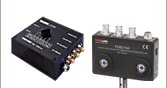
- Replacement Power Supply for the Balanced Amplified Photodetectors Sold Above
- ±12 VDC Power Output
- Current Limit Enabling Short Circuit and Overload Protection
- On/Off Switch with LED Indicator
- Switchable AC Input Voltage (100, 120, or 230 VAC)
- 2 m (6.6 ft) Cable with LUMBERG RSMV3 Male Connector
- UL and CE Compliant
The LDS12B ±12 VDC Regulated Linear Power Supply is intended as a replacement for the supply included with our PDB line of balanced photodetectors sold on this page. The cord has three pins: one for ground, one for +12 V, and one for -12 V (see diagram above). This power supply ships with a location-specific power cord. This power supply can also be used with the PDA series of amplified photodetectors, PMM series of photomultiplier modules, APD series of avalanche photodetectors, and the FSAC autocorrelator for femtosecond lasers.